Student Projects
Design of Power Management Chip for 6G communication applications
Project Video
Team Members

Team Members:
蔡润青 Runqing Cai 高景南 Jingnan Gao 顾珠江 Zhujiang Gu 黄昱程 Yucheng Huang 许海辰 Haichen Xu
Instructors:
Jigang Wu,Chengbin Ma
Project Description
-
Problem

Power Management Unit (PMU) is an important part for electronic devices due to its higher integration. The commonly-used PMU on the market, however, suffers from relatively high powerconsumption, large noise and lack of customized control. Our project is todesign a PMU with higher level of integration, low-power consumption, low-noise, smart control function and specific IO.
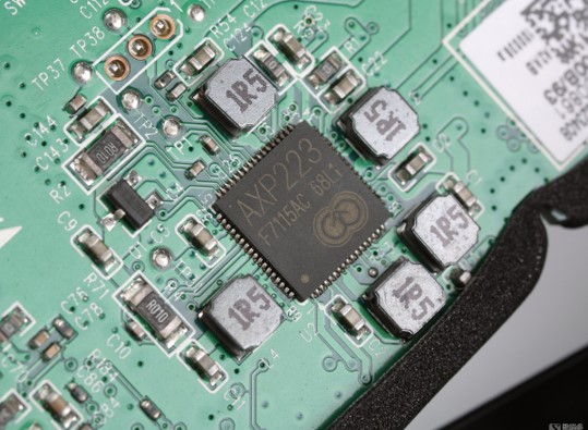
Fig. 1 Sample of PMU (AXP223) [1]
-
Concept Generation
The PMU consists of both digital and analog part. IO and ControlCircuit are included in digital part. Bandgap reference , linear dropout regulator and digital-to-analog convertor are required in analog part to generate reference voltage, stabilize power output and achieve adjustable output.
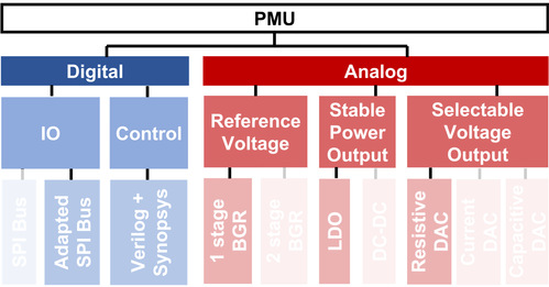
Fig. 2 Concept Diagram
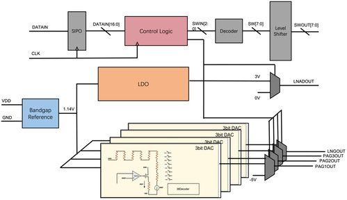
Fig. 3 System Diagram
-
Design Description
In order to satisfy the target, key components of the PMU are redesigned. Bandgap reference with novel structure is used to obtain stable reference voltage.Base on the process we use,we also deliberately design new operational amplifier which balances betweenthe power consumption, gain and gain bandwidth product. Additionally. The LDO we used in the PMU is designed to achieve the required stability and reaction speed. As for the DAC, we design the power-saving resistor string DAC with revised current mirror which fulfills the targeted speed of switching. Our overall design is shown in form of the layoutfigure below, the layout demonstrates the combination of each part as a whole in the chip.
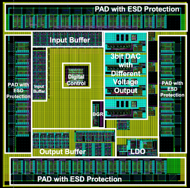
Fig. 4 Overall Layout
-
Validation
Validation Process:
The performance of each key component including PSRR and powerconsumption are simulated and tested individually. Temperature shift of BGR istested by sweeping its temperature curve, as well as PSRR. Open loop gain andphase margin of our LDO and gain bandwidth product of our Op-Amp are alsotested. For our DAC, switching time is simulated.
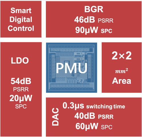
Fig. 5 Validation Result of Proposed PMU
-
Modeling and Analysis
Cadence virtuoso and Synopsys is used to simulate the circuit performance. Analog layout is drawn in Cadence virtuoso and digital layout is generated in Synopsys based on Verilogcode. The circuit models are provided from CSMC. The whole design is using its 180nm BCD process.

Fig. 5 Softwares used in this project
-
Conclusion
Based on CSMC 180nm BCD process, this 2 x 2 mm^2 power managementchip can generate specific low-noise voltage and power output with customized control up to 10 MHz. Performance including power consumption and PSRR can be further improved by redesigning key components and optimizing the power domain.
-
Acknowledgement
Instructor: Jigang Wu from UM-SJTU Joint Institute
Sponsor: Xuyang Lu from UM-SJTU Joint Institute
-
Reference
[1]AXP223 Power Mangement Chip. Photo taken by Soomal. www.soomal.com/pic/10100062618.htm